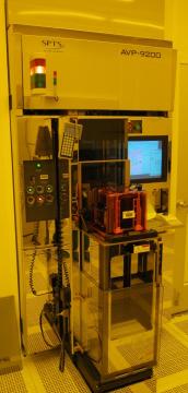
Integrated microsystems laboratory (MEMS) / Thermal treatment / Anneal
SPT Micro AVP-9200
CAPABILITY:
Thermal oxide thickness: 140 ± 6 nm, and 900 ± 20 nm
Within wafer thickness non-uniformity: 0.5% (1 sigma)
Wafer-to-wafer thickness non-uniformity: 0.4% (1-sigma)
Wafer size: 150 mm, 200 mm
Production wafers per load: 100
Thickness range of wafers: 300 – 1700 µm
Temperature range: 950°C – 1150 °C
Chamber configuration : Cross-flow
Gases used: Oxygen, Hydrogen, Nitrogen, TransLC
Mass flow control: ±5 sccm of the target gas flow
Annealing environment: Hydrogen/Oxygen
Wafer material: Silicon, Silicon-on-Insulator(SOI)


