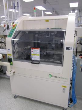
Packaging assembly laboratory / Component placement / Chip placement
Datacon EVO 2200
CAPABILITY:
JEDEC tray input/output
Accuracy +/- 10 µm @ 3 sigma, cpk 1.33
Theta axis rotary bond head 0˚ to 360˚ increments 0.0045˚
Theta placement accuracy +/- 0.15˚ @ 3 sigma
Automatic calibration function corrects thermal changes over time
Multi-chip placement in one single pass capability
Picking from wafer ( 4 to 12 in.) on 12 in. frame
(Or waffle pack / GEL PAK ( 2 x 2 in.)
Wafer table with stretcher
7 positions automatic tool changer unit
SECs/GEM capability
Wafer scanner and electronic wafer mapping capable
Pattern recognition system with edge, gray level, pattern and ink dot
Wafer size 50 to 300 mm
Frame size 375 mm
Die size 0.5 mm to 50 mm
Die thickness 0.05 to 7 mm


