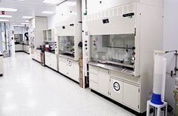
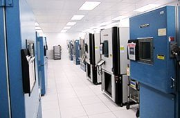
ANALYTICAL LABORATORY

The analytical laboratory plays a dual role within C2MI as it is contributing to both development support of new technologies / products / processes as well as to the development of uniformity control of the production processes over time. These analysis are performed to achieve a high quality standard for processes and products.
Failure analyses
The failure analysis can greatly help to solve problems of quality or reliability. These identify the underlying causes of these failures and help provide optimal corrective actions. Whether at the level of yield loss during manufacturing, to premature failure during reliability testing or customer return for a component not working properly, failure analyzes contribute to solving these problems. Several techniques are available to us to achieve this task.
ELECTRICAL CHARACTERIZATIONS:
Manual probing station
The probe station utilizes manipulators which allow the precise positioning of thin needles on the surface of a semiconductor device. The mechanical probe station is often used in the failure analysis of semiconductor devices, and for electrical characterization of semiconductor componants.
Resistivity measures (high precision multimeter)
Multimeter is an electronic measuring instrument that combines several measurement functions in one unit. A typical multimeter would include basic features such as the ability to measure voltage, current and resistance. The high precision multimeter offers the possibility to characterize low resistances by the 4-wire (Kelvin) connection method.
Leakage measures (pAmper-meter)
An ammeter or pAmper-meter is a measuring instrument used to measure small electrical current in a circuit. The pAmpermeter is able to characterize leakage current in the picoampere range, hence the name.
Capacitance measures (LCR meter)
Electronic equipment used to measure the inductance (L), capacitance(C), and resistance(R) of a passive component.
Impedance measures (VNA)
Parametric Network Analyzer (PNA) or Vector Network Analyzer (VNA) is an electronic equipment used to characterize linear and nonlinear component at low or high frequency (10MHz to 67GHz).
Parameter measures (VNA)
The parametric network analyzer (PNA) or vector network analyzer (VNA) is an electronic equipment used to characterize the linear and non-linear components at high or low frequency (10 MHz to 67GHz).
Dielectric constant measures (VNA)
Parametric Network Analyzer (PNA) or Vector Network Analyzer (VNA) is an electronic equipment used to characterize linear and nonlinear component at low or high frequency (10MHz to 67GHz).
Electrical continuity (curver tracers)
Curve tracer is an electronic test equipment used to stimulate the device under test (DUT). This equipment, based on an oscilloscope, can be used to analyze the characteristics of discrete semiconductor devices and to characterize the failure signature of a defective device.
NON-DESTRUCTIVE INSPECTION TECHNIQUES:
Time Domain Reflectory (TDR)
TDR is a non-destructive technique for IC package failure analysis. This technique sends a high frequency electrical pulse into the defective circuit in order to detect impedance variations related to the defect in the device under test (DUT), allowing to locate the defect.

3D Tomography: Defect C4
Non-destructive inspection technique using ultrasound waves to produce layer interface images in a package. Used in microelectronic to detect packaging defects, such as delamination, porosity, cracked chip..
3D tomography X-Ray

Non-destructive inspection technique using the X-Rays to produce 3D reconstruction image of a specific area of the scanned object. This technique is used to perform virtual slices of the scanned area allowing to see inside without cutting.
2D Real-Time X-Ray

Non-destructive inspection technique using the X-Rays to see inside of an object. Used in microelectronic to detect bond and assembly defects, such as missing wire, solder bridge and bad device positioning.
Surface analyses
Surface analysis are used both for the crystallographic characterization, inspection at high magnification, the elemental composition as determining the cleanliness of a surface or the thickness of an oxide. These analyzes are essential to the understanding of failures for adhesion problems, wettability or premature mechanical failures:
Scanning Electron Microscopy (SEM)
Electron microscope produces surface images (low & high magnification) of a sample by scanning it with a focused beam of electrons. The electron interact with atoms in the sample, producing various signals that can be detected. According detector used, information about the sample’s surface (SE detector), microstructure (EBSD) and composition (BSE & EDS) can be obtained.
Electron Backscatter Diffraction (EBSD)
Electron backscatter diffraction (EBSD), also known as backscatter Kikuchi diffraction (BKD) is a microstructural-crystallographic technique used to examine the crystallographic orientation of many materials, which can be used to elucidate texture or preferred orientation of any crystalline or polycrystalline material.
X-Ray Photoelectron Spectroscopy (XPS)
XPS, also known as ESCA (Electron Spectroscopy for Chemical Analysis), is a surface chemical analysis technique that can be used to analyze the surface chemistry of a material in its as-received state, or after some treatment. The X-Rays interact with the sample surface, giving a molecular chemical analysis of material present at the first atomic layers.
Contact Angle Goniometer
Goniometer is used to measure the contact angle through the liquid, where a liquid/vapor interface meets a solid surface. It quantifies the wettability of a solid surface by a liquid via the Young equation.
Auger Electron Spectroscopy (AES)
Type of scanning electron microscope used specifically in the study of the first atomic layers of a sample. This technique can be used to characterize the elemental chemical composition and determine the composition thickness of the top surface, such as oxide thickness.
Optical microscopes
Optical microscopes
Surface analysis
Failure analysis
Mechanical testing
Chemical analysis
Thermal analysis
Non-destructive inspection
Microsectioning
Etch Facilities
RELIABILITY LABORATORY

Technological pressures on the entire electronics industry constantly aim to reduce the size and cost of the transistor while increasing the amount of transistors per chip. However, those deemed critical expectations go against the long-term product reliability. To ensure product reliability over a period of life, the industry has implemented standardized tests. These tests are required to qualify new products and processes and thus control product consistency by simulating the life of products in an accelerated mode.
Mechanical stress
These tests are designed to ensure the functionality of the piece in the event of various impacts or vibrations between the first level assembly (module) and the second (attachment to the card) and when the piece is in use.
- Vibration
- Impact shock
Post stress integrity validation
Various checks are performed after stress to ensure the piece did not suffer significant damage that could impact its integrity and functionality.
- Open/short test
- Functional test
- Scanning acoustic microscopy
Environmental stresses
These tests expose the piece to one or more environmental conditions (temperature, humidity, pressure, etc.) for a given time which aims to simulate the conditions of application of the piece or to compare the robustness of different materials to such stress.
- Preconditionning
- Dtc/atc (thermal cycling)
- Thb (temperature, humidity, bias voltage)
- Pct (unbiased autoclave)
- Hast (highly accelerated stress test)
- Moisture resistance
- Hts (high temperature storage)

