Card Assembly / Paste inspection / Inspection
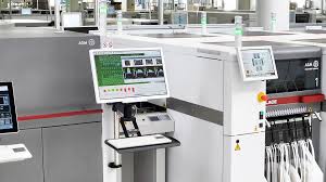
ASM ProcessLens
When defects related to the printing of the selected paste or media are seen by the inspection equipment, the corrections are directly transmitted to the printer without human intervention. The ASM ProcessLens solder paste printing behavior analysis system automatically learns, analyzes and optimizes printing parameters. After the automatic transfer of the part from the printer to the ASM ProcessLens, the latter measures the solder paste in 5D (3D + 2D), reads and analyzes the characteristics of the pattern of paste deposited.
Spécifications PCB:
PCB Size: 50 X 50 mm (2 x 1.59 in.) to 610 X 560.5 mm (24 X 22 in.).
PCB Thickness: 0.5 X 4.5 mm.
Minimum PCB edge clearance: 3 mm.
Underside PCB clearance: 25 mm.
Capacité d’inspection:
Pixel size (camera resolution): 15 x 15 μm
Inspection speed: Up to 30 cm2/s
Height resolution: 0.37 μm
Height accuracy: <= 2 μm (on calibration target).
X/Y gantry accuracy: < ±25 μm at 6 σ
Capacité d’inspection de la pâte de soudure:
Measurement: Shadow-free
Paste measurement functions: Volume, area, height, X-and Y-offset, shape, bridging, coplanarity
Maximum paste height: 1000 μm
Minimum paste size: 90 x 130 μm
Minimum paste pitch: 75 μm
Height repeatability on solder paste: <= 1 μm at ± 3 σ
Volume repeatability on solder paste: <= 3 % at ± 3 σ
Area repeatability on solder paste: <= 3 % at ± 3 σ
Gage Repeatability and Reproducibility (GRR): < 10 %


