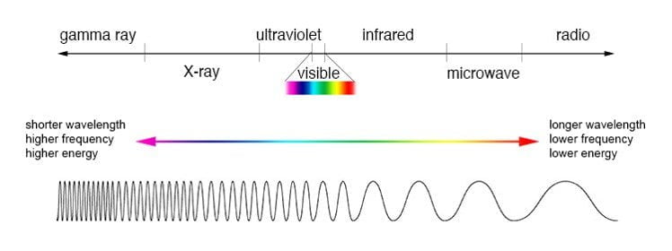
Did you know that the human eye is not sufficient to inspect the various stages of electronic products fabrication? Even using high magnifications to inspect the small structures, the eye, sensitive only to the visible light spectrum, fails to see many types of defects during fabrication. Inspection systems with detectors in different wavelengths are therefore used to inspect in Infra-Red, X-Ray and even using acoustic waves (between 10 and 300 Mega Hertz). The signal obtained by these tools is converted back to a shade of colors visible to the eye and makes it possible to identify defects in various interfaces. This is how the wafers bond interfaces are inspected with an infrared detector that “sees” through silicon wafers. This technique is also used to align patterns on either side of the wafer using alignment features present only on one side.


