3D interconnects could shorten delays within processor cores
Chipmaker GlobalFoundries (GF) and semiconductor IP firm Arm say they’ve completed the design for a test silicon 3D chip using technology capable of making a million 3D connections per square millimeter. Their technology binds two wafers of chips together with densely packed vertical copper links. The companies see it as a path to boosting the movement of data for applications such as machine learning, and to allowing the integration of different technologies such as RF and silicon photonics.
“We’ve done many years of hypothetical research into what we can do within Arm IP when interconnect density gets high enough,” says Greg Yeric, research fellow at Arm, in Austin, Texas. The company predicted that once 3D connections could be made 10 micrometers apart or less, designers would be able to use 3D connections to shorten the “critical path” in a processor core. That’s the path that creates the longest signal delay and therefore limits performance. The vertical connections allow the critical path to be folded up to flow from one silicon die to the other. GF’s technology has now reached that threshold.

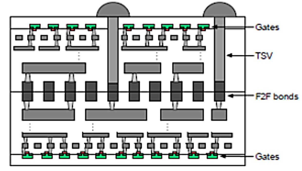
The technology is called “face-to-face” wafer-to-wafer bonding. Using this method, the system is designed in two parts and built on two wafers. One of the wafers includes vertical connections called through-silicon vias (TSVs) that extend down some distance into the body of the silicon. As usual in CMOS technology, the interconnects that bind the transistors into circuits are built in several layers above the silicon, but for wafer-to-wafer bonding, the top layer includes a dense array of bonding sites. The wafers are carefully aligned and bonded together face to face. Then enough of the silicon is removed from the back side of the wafer with the TSVs so that those connections are revealed. The 3D chips are then diced up and packaged.
The test chip the two companies have now designed is intended, first, to determine how well Arm’s mesh interconnect technology works in 3D. This will allow them to nail down a set of metrics for product development teams. They’ll be testing the silicon in early 2020.
Both GF and Arm engineers agree that the most difficult part of getting to this point was the lack of electronic design automation (EDA) tools capable of this kind of 3D design. The team has been working with Georgia Tech professor Sung Kyu Lim to enable 3D designs using 2D EDA tools. They’re also working with EDA tool makers, which Yeric would not name.

Adding to the design complexity, the team tried to incorporate IEEE’s draft “design for test” standard (IEEE p1838). Arm and GlobalFoundries want to be able to test the dies on the wafers both before and after bonding to ensure a good yield of working 3D chips. Much of this project “was an effort toward getting the design ecosystem ready,” says Arm principal research engineer Saurabh Sinha.
“Our goal here is to enable companies like Arm, and other customers, to be able to scale to high volume once the tools are in the tool box,” says John Pellerin, chief technologist, platforms, and vice president for worldwide R&D at GlobalFoundries.


