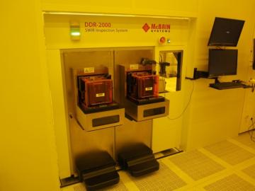
Integrated microsystems laboratory (MEMS) / Metrology / Inspection Infrared: multilayer and overlay measurement
McBain DDR2000 SWIR
Supplier :
Model :
Purpose :
Infra-Red Monitoring of the alignment/lateral dimension and defects inside bonded wafer stacks
CAPACITY:
Wafer size: 200 mm
Thickness range of wafers: 300 – 1700 µm
Wafer types: Silicon, Glass, Bonded Si-to-Si wafer stacks, Bonded Si-to-Glass stacks
Bonding interface overlay measurement
Bonding voids inspection
Multilayer overlay measurements
Lateral dimension inside wafer stacks
Inside cavity or TSV defect inspection
Wafer stress imaging by Scanning Infrared Depolarization (SIRD)
Infra-Red inspection and metrology of perforated wafers


