Integrated microsystems laboratory (MEMS) / Thin film deposition / Low pressure chemical vapour deposition / ISDP
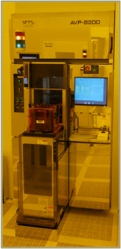
SPT AVP-8200 ISDP
CAPABILITY:
Film thickness: 330 ± 15 nm, 1550 ± 50 nm, and 2050 ± 75 nm
Within wafer thickness non-uniformity: 2.5% (1 sigma)
Wafer-to-wafer thickness non-uniformity: 2.5% (1-sigma)
Wafer size: 150 mm, 200 mm
Production wafers per load: 100 – 150
Thickness range of wafers: 300 – 1700 µm
ISDP deposition rate: 3.2 nm/min
Temperature range: 500 – 600 °C
Chamber configuration : Cross-flow
Gases used: Silane, Phosphine, Nitrogen
Silane mass flow control: ±0.5 sccm of the target flow-rate.
Phosphine mass flow control: ±0.1 sccm of the target flow-rate.
Automated in-situ clean using nitrogen trifluoride


