CAPABILITY: Electronic wafer map Conversion to make software compatible with ALPS wafer map Wafer expending film frame or ring holder
CAPABILITY: Electronic wafer map Conversion to make software compatible with ALPS wafer map Wafer expending film frame or ring holder

CAPACITÉ: Lampe UV multi faisceaux de 365nm Rainure simple passe de 60 µm de large Capacité d’épaisseur d’échantillon jusqu’à 1.5mm

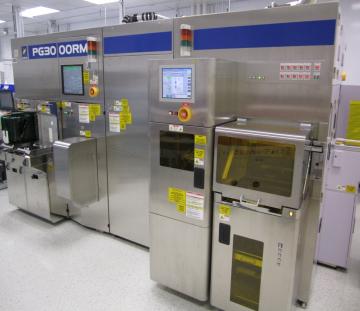
CAPACITY: Automatic slice support: 200 and 300mm Thickness from 800µm to 190µm Maximum number of bump / slice: 10 million
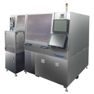
CAPABILITY: Ultra-thin automated wafer handling Automatic peeling and dicing frame (FF123) mounting Chemical/Mechanical polishing station 0.15 µm roughness TTV without
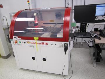
CAPACITÉ: Ajustement manuel de la tranche et de son cadre Application du film, découpe et retrait de l’excédent en mode
CAPACITY: Slices up to 300mm Positioning accuracy x, y axes: center offset ± 0.3mm Planar orientation axe axis: offset ±
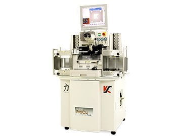
CAPACITY: Fully automatic flip chip bonder with chip supply unit 3D die bonding Chip on wafer (12 inch) Flux, NCP,
CAPABILITY: Fully automatic wire bonder Cassette in/out Typical ultra-fine pitch ball grid array product 35µm minimum pad pitch 2µm @
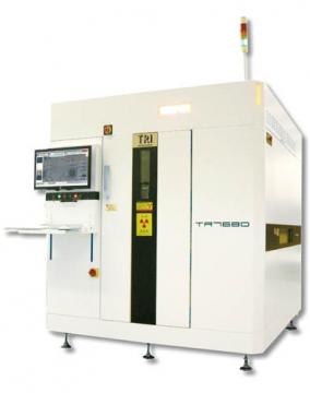
CAPABILITY: Multiple angle cameras provide 3D +2D images Maximum coverage, throughput and reliability with 3D Digital Tomosynthesis Imaging Technology Ideal
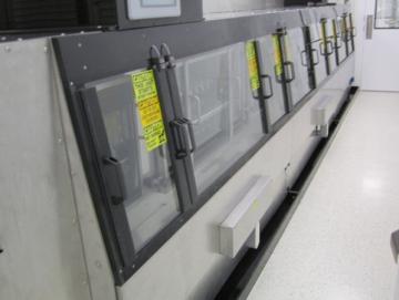
CAPABILITY: Conveyor belt stainless steel 24 ‘’ wide, 0.072 ‘’ wire x 3/8 ‘’ pitch 2 Jedec conveyor lane Adjustable
En naviguant sur notre site, certains témoins peuvent être conservés dans votre navigateur ou récupérés à partir de celui-ci. Ces informations peuvent porter sur vous, vos préférences ou votre appareil et sont principalement utilisées pour s'assurer que le site fonctionne correctement. Les informations ne permettent pas de vous identifier directement, mais peuvent vous permettre de bénéficier d'une expérience Web améliorée. Parce que nous respectons votre vie privée, nous vous donnons l'opportunité de ne pas autoriser ces témoins.

En naviguant sur notre site, certains témoins peuvent être conservés dans votre navigateur ou récupérés à partir de celui-ci. Ces informations peuvent porter sur vous, vos préférences ou votre appareil et sont principalement utilisées pour s'assurer que le site fonctionne correctement. Les informations ne permettent pas de vous identifier directement, mais peuvent vous permettre de bénéficier d'une expérience Web améliorée. Parce que nous respectons votre vie privée, nous vous donnons l'opportunité de ne pas autoriser ces témoins.