SEMICONDUCTOR ASSEMBLY LABORATORY

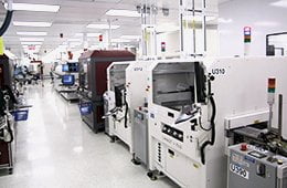
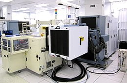
C2MI offers a wide range of equipment to conduct the advanced packaging of semiconductors as a finished product on a substrate ready for assembly to the card. The integrated circuit (IC), also called electronic chip is an electronic component reproducing one or more electronic function more or less complex, often incorporating several basic types of electronic components in a small volume, making it easy to circuit work. There is a wide variety of these components divided into two categories: analog and digital.
Wafer cutting
A chip is a small piece of semiconductor on which an electronic integrated circuit was manufactured. The chips are obtained by cutting semiconductor wafers on which is this electronic circuit obtained by a succession of steps of photolithography, ion implants, thin film deposition or even more electronic circuits.
The term “chip” is used when the manufacturing process is completed and which has been performed the cutting of the semiconductor wafer.
C4 assembly
The bearings (connection with a solder alloy on a plot) are at the heart of the chip connection technologies reversed (flip chip). The electrical connection between the chip and the substrate on which they are assemble is provided by the presence of a conductive microbead on a layer called UBM (Under Bump Metallurgy) that bridges the microbead and the semiconductor circuit. The “Flip Chip” assembly method is therefore to assemble this chip with microbeads on a substrate from a positioning method and a temperature cycle carefully controlled. The assembly recipe is influenced by many settings and components (the UBM, the solder alloy, the kind of substrate, etc.).
Wirebond assembly
The assembly technique of the binding thread (wirebond) is the method of making interconnections usually used between an integrated circuit (IC) and another device which serves as a support. The wire bonding technique is generally regarded as the most cost effective and flexible interconnect technology, and is still used today to assemble the vast majority of semiconductor devices.
Others
Wirebond assembly
Wafer Dicing
Balling
Underfill
Component placement
Lid attach
Metal deposition
Inspection
Marking
ELECTRICAL TESTING LABORATORY

C2MI can perform several types of electrical testing. Electrical tests are performed to ensure the quality and reliability of long-term devices or for collection purposes to eliminate the few devices that are failing or measure and collect information on changes induced by radiation in the characteristics of the component.
Functionality tests
The functionality test aims to eliminate the bad processes in a limited period of time to spare the costs as much as possible. On modern testers, components found on modern testers are tested with a higher parallelism. In other words, components are increasingly tested simultaneously. So, it almost possible to divide the test of time by the number of components in parallel. There is another method to reduce the test time. This is to adapt the component itself in DFT test.
During the test, the components are commonly manipulated by machines called “Handler”. Some handlers used to test components at higher or lower temperatures than the room. This ensures the functionality of the part in a wide range of temperature.
Package automated inspection
Automated interconnection mechanical inspection verifies the integrity of the piece, ensuring that it meets customer specifications.
Artificial weathering test
All electronic components are experiencing failures during their lives. Thus, once they have survived for some time, the chances of recurrence are low. Submit components to conditions of extreme temperature and aging can accelerate the onset of their manufacturing defects and ensure proper system operation.
Application engineering
The engineering department offers complete solutions for electrical tests from design to production.
- Participation in the application design
- Planning of the testing strategy including several design for test techniques
- Selection of test equipment and test card design
- Redaction of the test program, including the conversion of test vectors
- Prototypes characterization
- Optimization and production

Test program development
Our experienced technical staff provides a full range of services, including test program development. We understand the different applications and testing requirements, including digitals applications, mixed-signal, high speed, RF, and emerging technologies like 2.5 / 3D and SiPh.
From the test specifications, the test engineer will develop a test sequence to optimize the product quality, performance and cost.
Manufacturing solutions
Mass production is a critical step in the product’s life cycle. Throughout the development of the test solution, the engineering team considers the automated solution that will be used in mass production and set up all the tools necessary for this transition. Here is our expertise in manufacturing solutions:
- Fully automated solutions
- Multi-site programming
- Lot management logistics
- Returns and Maverick lots management
- Capacity management
- Test equipment management
- Static analysis
- Mathematical modeling
- Data Mining
- Expert systems
- Customer returns management
- Test programs updates
- Testing time reduction during product’s life
Others
- Migration of test program on different testers
- Test vectors conversion
- Burnin (products aging)
- Application’s specific solution (on board test fixturing)
- System level Test

